






















Service Hotline
News

News
For radio frequency chips, this article is enough!
2021-12-28
766
A mobile phone that can support calls, text messages, network services, and APP applications usually contains five parts:RF, baseband, power management, peripherals, software. Complete receiving and transmitting switching; Complete 900M/1800M signal reception switching. Amplify the weak current induced by the antenna to meet the signal amplitude requirements of the subsequent circuit. Complete 900M/1800M receiving signal switching. powered by:The base bias voltages of the two high-amplifier tubes of 900M/1800M share one channel, which is provided by the IF simultaneous channel; and the bias voltage of the collectors of the two tubes is sent out by the IF CPU in two channels according to the reception status of the mobile phone. Its purpose is to complete the switching of 900M/1800M receiving signals. After filtering out other clutter through the filter, the pure 935M-960M received signal is coupled by a capacitor and sent to the corresponding high-amplifier tube for amplification and then sent to the intermediate frequency through the capacitor coupling for subsequent stage processing.
RF:Generally the part where information is sent and received;
Baseband:Generally it is the information processing part;
Power management:Generally, it is the power saving part. Since mobile phones are devices with limited energy, power management is very important;Peripherals:Generally includes LCD, keyboard, case, etc.;software:Generally includes systems, drivers, middleware, and applications.
In mobile phone terminals, the most important cores are radio frequency chips and baseband chips.The radio frequency chip is responsible for radio frequency transceiver, frequency synthesis, and power amplification; the baseband chip is responsible for signal processing and protocol processing.So what is the relationship between RF chips and baseband chips?
The relationship between RF chips and baseband chips
Radio frequency (Radio Frenquency) and baseband (Base Band) are both literal translations from English.Among them, the earliest application of radio frequency is Radio - wireless broadcast (FM/AM). So far, this is still the most classic application of radio frequency technology and even the radio field.
The baseband is the signal with the band center point at 0Hz, so the baseband is the most basic signal.Some people also call baseband "unmodulated signal". This concept used to be correct. For example, AM is a modulated signal (no modulation is required, and the content can be read through the sound-generating component after reception).
But in the field of modern communications, baseband signals usually refer to digitally modulated signals with the center point of the spectrum at 0Hz.And there is no clear concept that the baseband must be analog or digital. It all depends on the specific implementation mechanism.
Closer to home, the baseband chip can be considered to include the modem, but it is not limited to the modem, but also includes channel codec, source codec, and some signaling processing.The radio frequency chip can be regarded as the simplest up-conversion and down-conversion of the baseband modulation signal.
The so-called modulation is the process of modulating the signal to be transmitted onto the carrier according to certain rules and then sending it out through the wireless transceiver (RF Transceiver). Demodulation is the opposite process.
Working principle and circuit analysis
Radio frequency, referred to as RF, refers to radio frequency current, which is a high-frequency alternating electromagnetic wave. It is the abbreviation of Radio Frequency, which represents electromagnetic frequencies that can be radiated into space. The frequency range is between 300KHz and 300GHz.Alternating current that changes less than 1,000 times per second is called low-frequency current, and alternating current that changes more than 10,000 times is called high-frequency current, and radio frequency is such a high-frequency current.High frequency (greater than 10K); radio frequency (300K-300G) is the higher frequency band of high frequency; microwave frequency band (300M-300G) is the higher frequency band of radio frequency.Radio frequency technology is widely used in the field of wireless communications, and cable television systems use radio frequency transmission.
A radio frequency chip refers to an electronic component that converts radio signal communication into a certain radio signal waveform and sends it out through antenna resonance. It includes a power amplifier, a low-noise amplifier and an antenna switch.The radio frequency chip architecture includes two parts: the receiving channel and the transmitting channel.
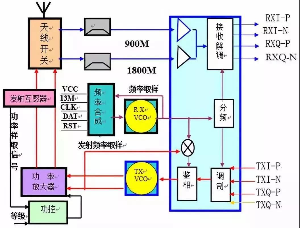
RF circuit block diagram
The structure and working principle of the receiving circuit
When receiving, the antenna converts the electromagnetic wave sent by the base station into a weak AC current signal, which is filtered, amplified at high frequency, and sent to the intermediate frequency for demodulation to obtain the received baseband information (RXI-P, RXI-N, RXQ-P, RXQ-N); it is sent to the logic audio circuit for further processing.
This circuit masters the key points:
1. Receiver circuit structure;
2. The functions and functions of each component;
3. Receiving signal process.
Circuit structure
The receiving circuit is composed of antenna, antenna switch, filter, high-amp tube (low-noise amplifier), intermediate frequency integrated block (receiving demodulator) and other circuits.Early mobile phones had primary and secondary mixing circuits, whose purpose was to reduce the receiving frequency and then demodulate it (as shown in the figure below).
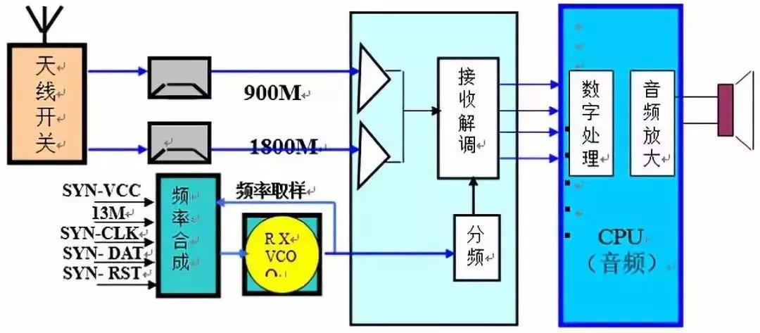
Receiver circuit block diagram
2. Functions and functions of each component
1). Mobile phone antenna:structure:(pictured below)Mobile phone antennas are divided into two types: external and internal antennas; they are composed of an antenna base, a solenoid, and a plastic envelope.
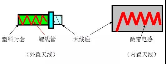
a) When receiving, the electromagnetic waves sent by the base station are converted into weak AC current signals.
b) When transmitting, the AC current amplified by the power amplifier is converted into an electromagnetic wave signal.
2), Antenna switch:
structure:(pictured below)The mobile phone antenna switch (combiner, duplex filter) consists of four electronic switches.
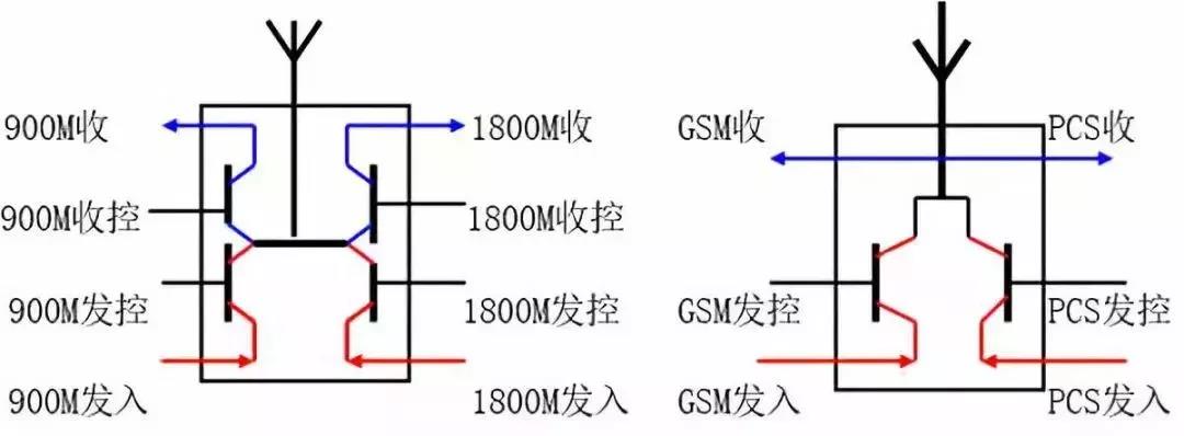
The logic circuit sends out control signals (GSM-RX-EN; DCS-RX-EN; GSM-TX-EN; DCS-TX-EN) respectively according to the working status of the mobile phone, so that the respective channels are turned on, so that the receiving and transmitting signals go their own way without interfering with each other.
Because the mobile phone cannot work in the same time slot when receiving and transmitting at the same time (that is, it does not transmit when receiving and does not receive when transmitting).Therefore, later new mobile phones removed the two switches in the receiving path, leaving only two transmitting switches; the receiving switching task was completed by the high-amplifier tube.
3), filter:
structure:There are high-frequency filters and medium-frequency filters in mobile phones.effect:Filter out other useless signals and obtain pure received signals.Later new mobile phones are all zero-IF mobile phones; therefore, there is no IF filter in the mobile phone.
4), high amplifier tube (high frequency amplifier tube, low noise amplifier):
structure:
There are two high-amplifier tubes in mobile phones:900M high discharge tube, 1800M high discharge tube.They are all triode common-emitter amplifier circuits; later new mobile phones integrated high-amplifier tubes inside the intermediate frequency.
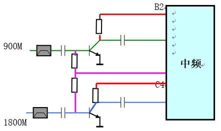
High frequency amplifier tube power supply diagram
principle:
5), IF (RF interface, RF signal processor):
structure:It is composed of receiving demodulator, transmit modulator, transmit phase detector and other circuits; the new mobile phone also integrates high-amplifier tube, frequency synthesis, 26M oscillation and frequency division circuit inside (as shown below).
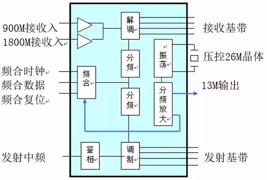
a) The internal high-amplifier tube amplifies the weak current induced by the antenna;
b) When receiving, demodulate the received carrier frequency signal (with counterpart information) of 935M-960M (GSM) and the local oscillator signal (without information) to obtain the received baseband information of 67.707KHZ;
c) When transmitting, modulate the transmit information processed by the logic circuit and the local oscillator signal into a transmit intermediate frequency;
d), combine 13M/26M crystal to generate 13M clock (reference clock circuit);e) Based on the reference signal sent by the CPU, a local oscillator signal that conforms to the working channel of the mobile phone is generated.
3. Receiving signal process
When the mobile phone is receiving, the antenna converts the electromagnetic wave sent by the base station into a weak AC current signal, which passes through the antenna switch receiving path and is sent to a high-frequency filter to filter out other useless clutter to obtain a pure 935M-960M (GSM) received signal, which is coupled into the intermediate frequency by a capacitor. After amplification by the corresponding high-amplifier tube, it is sent to the demodulator to demodulate the local oscillator signal (without information) to obtain the 67.707KHZ receiving baseband information (RXI-P, RXI-N, RXQ-P, RXQ-N); it is sent to the logic audio circuit for further processing.
The structure and working principle of the transmitter circuit
When transmitting, the transmit baseband information processed by the logic circuit is modulated into a transmit intermediate frequency, and the TX-VCO is used to change the frequency of the transmit intermediate frequency signal into a frequency signal of 890M-915M (GSM).After being amplified by the power amplifier, it is converted into electromagnetic waves and radiated by the antenna.
This circuit masters the key points:
(1), circuit structure;
(2) The functions and functions of each component;
(3). Transmitting signal process.
Circuit structure
The transmit circuit is composed of the transmit modulator, transmit phase detector, transmit voltage controlled oscillator (TX-VCO), power amplifier (power amplifier), power controller (power control), transmit transformer and other circuits inside the intermediate frequency.(pictured below)
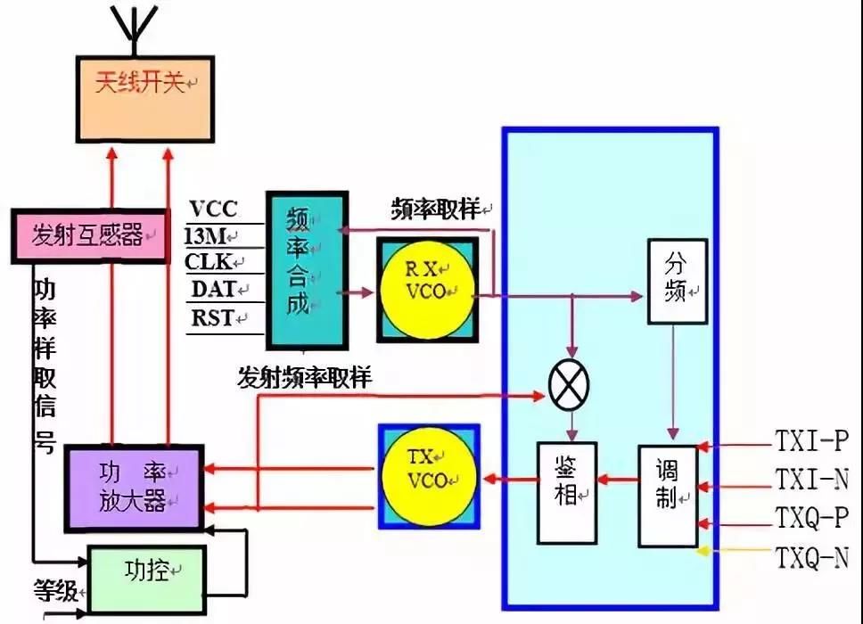
Transmitter circuit block diagram
1). Transmit modulator:structure:The transmit modulator is inside the IF, which is equivalent to the MOD in the broadband network.effect:During transmission, the transmission baseband information (TXI-P; TXI-N; TXQ-P; TXQ-N) processed by the logic circuit and the local oscillator signal are modulated into a transmission intermediate frequency.
2). Transmit voltage controlled oscillator (TX-VCO):structure:The transmitting voltage controlled oscillator is a capacitive three-point oscillator circuit whose output frequency is controlled by voltage; it is integrated into a small circuit board during production and leads to five pins:Power supply pin, ground pin, output pin, control pin, 900M/1800M frequency band switching pin.When there is a suitable working voltage, it will oscillate and generate a corresponding frequency signal.
effect:Convert the transmitted IF signal modulated by the IF modulator into the 890M-915M (GSM) frequency signal that the base station can receive.
principle:As we all know, the base station can only receive frequency signals of 890M-915M (GSM), but the base station cannot receive the IF signal modulated by the IF modulator (such as Samsung transmitting an IF signal of 135M). Therefore, a TX-VCO is used to change the frequency of the transmitted IF signal to a frequency signal of 890M-915M (GSM).
When transmitting, the power supply section sends out 3VTX voltage to make the TX-VCO work, generating a frequency signal of 890M-915M (GSM) in two ways:
a) The sample is sent back to the internal IF, mixed with the local oscillator signal to produce a transmit frequency discrimination signal equal to the transmit intermediate frequency, and sent to the phase detector for comparison with the transmit intermediate frequency; if the oscillation frequency of the TX-VCO does not match the working channel of the mobile phone, the phase detector will generate a 1-4V jump voltage (DC voltage with AC transmit information) to control the capacitance of the varactor diode inside the TX-VCO to achieve the purpose of adjusting the frequency accuracy.
b) After being amplified by the power amplifier, it is converted into electromagnetic waves and radiated out by the antenna.
It can be seen from the above:The frequency generated by TX-VCO is sampled and sent back to the IF, and then the voltage is generated to control the operation of TX-VCO. It just forms a closed loop and controls the frequency phase, so this circuit is also called a transmit phase-locked loop circuit.
3), power amplifier (power amplifier):
structure:At present, the power amplifier of mobile phones is a dual-band power amplifier (900M power amplifier and 1800M power amplifier integrated into one), which are divided into two types: vinyl power amplifier and iron case power amplifier; different models of power amplifiers cannot be interchanged.
effect:Amplify the frequency signal oscillated by the TX-VCO to obtain sufficient power current, which is converted into electromagnetic waves by the antenna and radiated out.
Worth noting:The power amplifier amplifies the amplitude of the transmitted frequency signal, not its frequency.
Working conditions of power amplifier:
a), working voltage (VCC):The mobile phone amplifier is powered directly by the battery (3.6V);
b), ground terminal (GND):causing current to form a loop;
c), dual-frequency power conversion signal (BANDSEL):Control the power amplifier to work at 900M or 1800M;
d), power control signal (PAC):Control the amplification amount (operating current) of the power amplifier;
e), input signal (IN); output signal (OUT).
4). Transmitting transformer:structure:Two coils with equal wire diameter and number of turns are placed close to each other and are composed using the principle of mutual inductance.effect:Send the power amplifier transmit power current sample to the power control.principle:When the transmitter power current of the power amplifier passes through the transmitter transformer during transmission, a current of the same size as the power current is induced on its secondary side, which is detected (high-frequency rectified) and sent to the power control.
5), power level signal:The so-called power level means that engineers divide the received signal into eight levels when programming the mobile phone. Each receiving level corresponds to a level of transmit power (as shown in the table below). When the mobile phone is working, the CPU determines the distance between the mobile phone and the base station based on the strength of the received signal, and sends an appropriate transmission level signal to determine the amplification amount of the power amplifier (that is, when the reception is strong, the transmission is weak).
Attached is the power level table:

effect:Compare the transmit power current sampling signal with the power level signal to obtain a suitable voltage signal to control the amplification amount of the power amplifier.
principle:When the power current passes through the transmitting transformer during transmission, the current induced in its secondary is detected (high-frequency rectification) and sent to the power control; at the same time, the preset power level signal during programming is also sent to the power control; the two signals are compared internally to generate a voltage signal to control the amplification amount of the power amplifier, so that the working current of the power amplifier is moderate, which not only saves power but also prolongs the service life of the power amplifier (the higher the power control voltage, the greater the power of the power amplifier).
3. Signal transmitting process
When transmitting, the transmit baseband information (TXI-P; TXI-N; TXQ-P; TXQ-N) processed by the logic circuit is sent to the transmit modulator inside the intermediate frequency, and modulated with the local oscillator signal into the transmit intermediate frequency.If the intermediate frequency signal base station cannot receive it, the TX-VCO must be used to increase the frequency of the transmitted intermediate frequency signal to 890M-915M (GSM) in order for the base station to receive it.When the TX-VCO is working, the frequency signal generated from 890M-915M (GSM) goes in two ways:
a) One channel of sampling is sent back to the internal IF, mixed with the local oscillator signal to produce a transmit frequency discrimination signal equal to the transmit intermediate frequency, and sent to the phase detector for comparison with the transmit intermediate frequency; if the oscillation frequency of the TX-VCO does not match the working channel of the mobile phone, the phase detector will generate a 1-4V jump voltage to control the capacitance of the varactor diode inside the TX-VCO to adjust the frequency.
b). The two-way input power amplifier is amplified and converted into electromagnetic waves by the antenna for radiation.In order to control the amplification amount of the power amplifier, when the power current passes through the transmitting transformer during transmission, the current induced in its secondary is detected (high-frequency rectification) and sent to the power control; at the same time, the preset power level signal during programming is also sent to the power control; the two signals are compared internally to generate a voltage signal to control the amplification amount of the power amplifier, so that the working current of the power amplifier is moderate, which not only saves power but also prolongs the service life of the power amplifier.
Current status of domestic RF chip industry chain
In the field of radio frequency chips, the market is mainly monopolized by overseas giants. In terms of domestic radio frequency chips, no company can independently support the IDM operating model, mainly Fabless design companies; domestic companies have formed a "soft IDM" operating model through collaboration in design, foundry, and packaging.
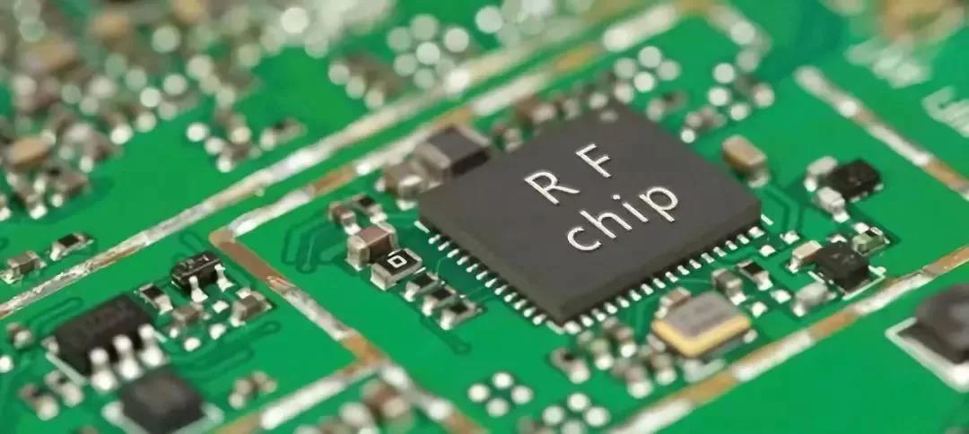
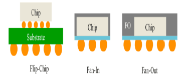
In terms of RF chip packaging, on the one hand, the frequency of 5G RF chips increases, which causes the connection wires in the circuit to have a greater impact on circuit performance. When packaging, the length of the signal connection wires needs to be reduced; on the other hand, the power amplifier, low-noise amplifier, switch and filter need to be packaged into a module. On the one hand, it reduces the size and on the other hand, it is convenient for downstream terminal manufacturers to use.In order to reduce the parasitics of RF parameters, Flip-Chip, Fan-In and Fan-Out packaging technologies need to be used.
When Flip-Chip is packaged with Fan-In and Fan-Out processes, there is no need for signal connections through gold wire bonding wires, which reduces the parasitic electrical effects caused by gold wire bonding wires and improves chip RF performance. In the 5G era, high-performance Flip-Chip/Fan-In/Fan-Out combined with Sip packaging technology will be the future packaging trend.
This content comes from the Internet/filter, this website only provides reprinting. The views, stance, technology, etc. of this article have nothing to do with this website. If there is any infringement, please contact us to delete it!
Related Recommendations